Most new technologies are driving the “MORE THAN MOORE” and the “MORE MOORE ” domains

Ion implantation, essential to those technologies, requires :
  • Higher doses at lower energies with high throughput
  • Implantation of 3D structures
  • Material modification i.e. use of ion implant for non doping applications (etch selectivity, contact improvement, patterning, layer synthesis, strain engineering, etc)
  • Hot implantation
  • Large range of species
  • Ion implantation tools must have :
  • High flexibility & versatility
  • High productivity
  • Easy maintenance
  • Low foot print
  • With 30 years of implant background, IBS is the only company that can offer both a range of new implant tools & full implant services.

    IBS PULSION equipment meet < 10 nm requirements

    Continued scaling of non-planar HP multigate devices in all aspects:
    EOT, junctions, mobility enhancement, new channel materials,
    parasitic series resistance, contact silicidation.

    • Materials compatibility

    • Process integration challenges

    PULSION®

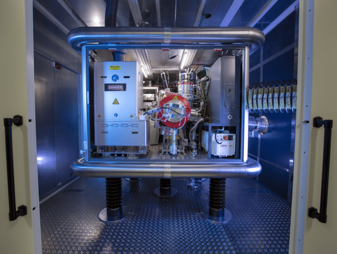
    Plasma immersion ion implantation is a versatile process
    technology with wide applications in microelectronics
    processing & materials engineering.
  • Offers
    Simultaneous implantation of the full wafer
    Ultra low energy ( down to 30 eV)
    Conformal 3D implantation
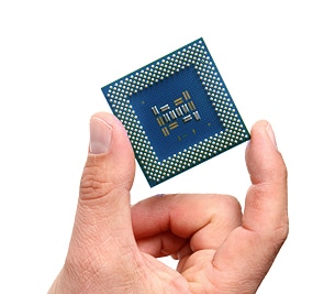
  • Ideal tool for
    3D doping (FINFET, DTI, pillars ...) for advanced logic & memory
    Material modification to tailor stress, to engineer contact & Vt, to help process integration
    Very high doses needed for DPG application
  • Medium current production implanter for:
    RF and power devices, sensors, opto-electronics manufacturing
    on Si, SiC, GaAs, GaN, LiTaO3, HgCdTe, LiNbO3, InP…

    FLEXion 200/400, FLEXion 400-SiC

    To fulfill manufacturer’s needs for compound Semiconductors
    and SiC components, IBS has designed a family of implanters avoiding
    the costly complexity of a 300 mm Si machine downgraded for SiC.
  • Key advantages
    High beam current
    Extended life ion source (>300 hrs)
    Enhanced single or multi-charged Al beam generation
    High resolution analyzer magnet for multi-charged and high AMU beams
    650 °C fast temperature ramp-up/ramp-down platen for SiC
    Optimized throughput for non Si materials
  • Features
    Quad implant, autotune up to 10 chained implantations
    From coupons to 200 mm, parallel scanning for 200 mm wafers
    Up to 1.2 MeV
    High efficiency ion sources (Indirect heated Cathode, ECR)
    Up to 8 different implant gases
  • SiC Devices PULSION® FOR POWER
    DEVICE APPLICATION
    COMPOUND
    SEMICONDUCTORS

    Silicon carbide (SiC): smaller, faster, more robust, this material will supplant silicon in converters for electrical vehicles, industrial motors and power grids.
    Manufacturing SiC components requires dedicated ion implantation tools.

    IMC advantages
    Implants up to 800 keV
    Intense current and stable Al beam
    High temperature platen
    PULSION® advantages
    Gate technology engineering for MOS SiC
    Contact doping improvement
    Customer requirements
    High temperature implantation
    Wafer handling for brittle materials
    PULSION® advantages
    High throughput at high doses and low energy
    Low-mechanical stress, stable single wafer platen for thinned wafers; reduced breakage
    Conformal trench sidewall doping (even for high aspect ratio).
    Customer requirements
    Similar doping results to beamline implantation
    Higher throughput and performance
    Possible lower energy control for advanced devices
    Applications
    Gate trench sidewall doping (low dose, conformal)
    Backside contact doping (high dose, after back thinning)

    Data communications, telecommunication systems and security
    require more and more compound semiconductors such as
    optoelectronics and RF amplifiers. Due to material and contamination
    concerns, a manufacturing line must operate with dedicated tools.

    IMC advantages
    400 kV beam line for implant up to 800 keV
    Gentle handling for brittle materials
    Wide range of implant species, among which: Be, Si, Mg, Cs, Yb...
    Typical applications
    HgCdTe IR sensor and imager
    InP laser
    VCSEL
    GaAs RF power amplifier and switches
    Power GaN power components